Appearance
RTL / VHDL
This first delivery is an introduction/warm-up to VHDL and FPGA, we will create a dedicated hardware on the FPGA to control the board's LEDs based on the input signals from the buttons. The idea is to go through the entire process of developing a hardware in FPGA and with VHDL.
Getting Started
To follow this tutorial you will need:
- Hardware: DE10-Standard and accessories
- Software: Quartus 25.01
- Documents: DE10-Standard_User_manual.pdf
Quartus
First, we must create a new project in the Quartus software.
Exercise
In Quartus: File ➡️New Project Wizard
- Directory, Name, Top-Level Entity
- Choose the destination as your repository. Name the project as
Lab1_FPGA_RTL
- Choose the destination as your repository. Name the project as
- Project Type
- Empty Project
- Add Files
- We won't add any files for now.
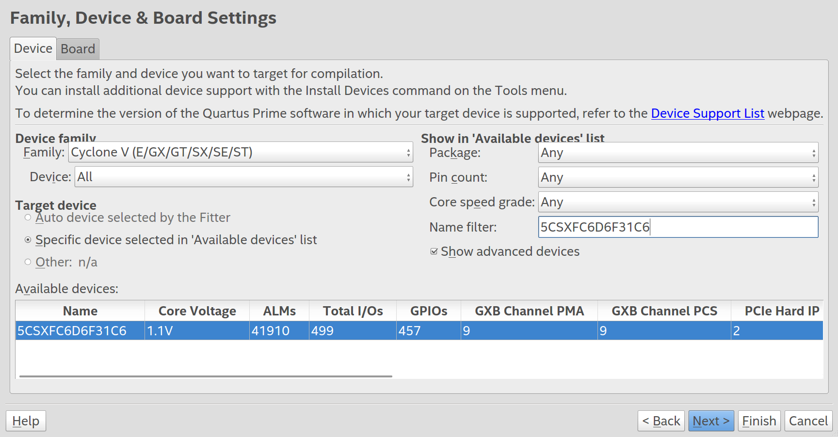
- Family, Device & Board Settings
- Look for the FPGA:
- Family:
Cyclone V - Name:
5CSXFC6D6F31C6
- Family:
- Look for the FPGA:
- 🆗 Finalize the Wizard
Other references
If you need other reference material, there's a Terasic tutorial: DE10-Standard_My_First_Fpga.pdf
Creating the topLevel
TopLevel is the name of the topmost module in hierarchical development where, generally, the entity signals (in/out,...) will be mapped to hardware pins (connection with the external world).
Exercise
Let's add a file to the newly created project:
File➡️New➡️VHDL FileFile➡️save as➡️- name:
Lab1_FPGA_RTL.vhd
- name:
- 🆗
toplevel source file
Initialize the file with the following content ( this code could be more elegant, but we'll keep it simple for the sake of understanding. )
vhdl
library IEEE;
use IEEE.std_logic_1164.all;

entity Lab1_FPGA_RTL is
    port (
        -- Gloabals
        fpga_clk_50   : in  std_logic;

        -- I/Os
        fpga_led_pio  : out std_logic_vector(5 downto 0)
  );
end entity Lab1_FPGA_RTL;

architecture rtl of Lab1_FPGA_RTL is

-- signal
signal blink : std_logic := '0';

begin

  process(fpga_clk_50)
      variable counter : integer range 0 to 25000000 := 0;
      begin
        if (rising_edge(fpga_clk_50)) then
                  if (counter < 10000000) then
                      counter := counter + 1;
                  else
                      blink <= not blink;
                      counter := 0;
                  end if;
        end if;
  end process;

  fpga_led_pio(0) <= blink;
  fpga_led_pio(1) <= blink;
  fpga_led_pio(2) <= blink;
  fpga_led_pio(3) <= blink;
  fpga_led_pio(4) <= blink;
  fpga_led_pio(5) <= blink;

end rtl;
Configuring the topLevel
In Quartus, we need to specify which entity is the topLevel. As VHDL does not define a standard for this, any entity can be configured as the top.
Exercixe
In Quartus:
Project➡️Set as Top-Level Entity
This command will set the current file as the topLevel of the project. Note that Quartus assigns the entity's name as the file's name to the topLevel. If for any reason (which happens) the file's name is not the same as the entity's, this will not work.
TIP
As we saved the file with the same name as the project and the entity has the same name as well, Quartus recognizes this entity as the TopLevel by default.
Verifying
Let's make sure everything is fine so far by doing a complete compilation of the project.
Exercise
To full complile the project on quartus:10000000
➡️ Processing ➡️ Start Compilation.
Please wait! Hardware compilations can take quite a long time.
I/Os
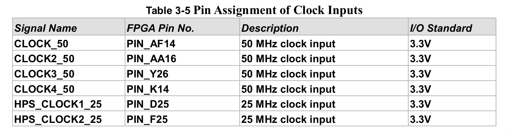
Remember that the topLevel is the entity that will be mapped with the external world. In this case, the signals: fpga_clk_50; fpga_led_pio; should be connected to the FPGA pins that are connected to these devices (50 MHz clock; Six LEDs).
Notice the error that Quartus generated when we asked it to compile the project ("Show Critical Warnings Messages"):
Failure
Critical Warning (169085): No exact pin location assignment(s)
for 6 pins of 6 total pins. For the list of pins please refer
to the I/O Assignment Warnings table in the fitter report.
This error indicates that from the topLevel 6 signals were not mapped to their corresponding pins.
Pins
We must indicate to the tool which pins and which signal standard it should use for each of the signals defined in the topLevel entity.
LEDs
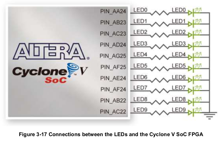
On page 22 of the board manual, we have the definitions of how the FPGA pins were used on the board:
There are also ten user-controllable LEDs connected to the FPGA. Each LED is driven directly and individually by the Cyclone V SoC FPGA; driving its associated pin to a high logic level or low level to turn the LED on or off, respectively. Figure 3-17 shows the connections between LEDs and Cyclone V SoC FPGA. Table 3-6, Table 3-7 and Table 3-8 list the pin assignment of user push-buttons, switches, and LEDs.
CLOCK
From the manual:
Figure 3-13 shows the default frequency of all external clocks to the Cyclone V SoC FPGA. A clock generator is used to distribute clock signals with low jitter. The four 50MHz clock signals connected to the FPGA are used as clock sources for user logic. One 25MHz clock signal is connected to two HPS clock inputs, and the other one is connected to the clock input of Gigabit Ethernet Transceiver. Two 24MHz clock signals are connected to the clock inputs of USB Host/OTG PHY and USB hub controller. The associated pin assignment for clock inputs to FPGA I/O pins is listed in Table 3-5.
Pin Assignment
We will use the Pin Planner to insert these pins informations.
Exercise
To edit the pin assgiments:
➡️ Assignments ➡️ Pin Planner.
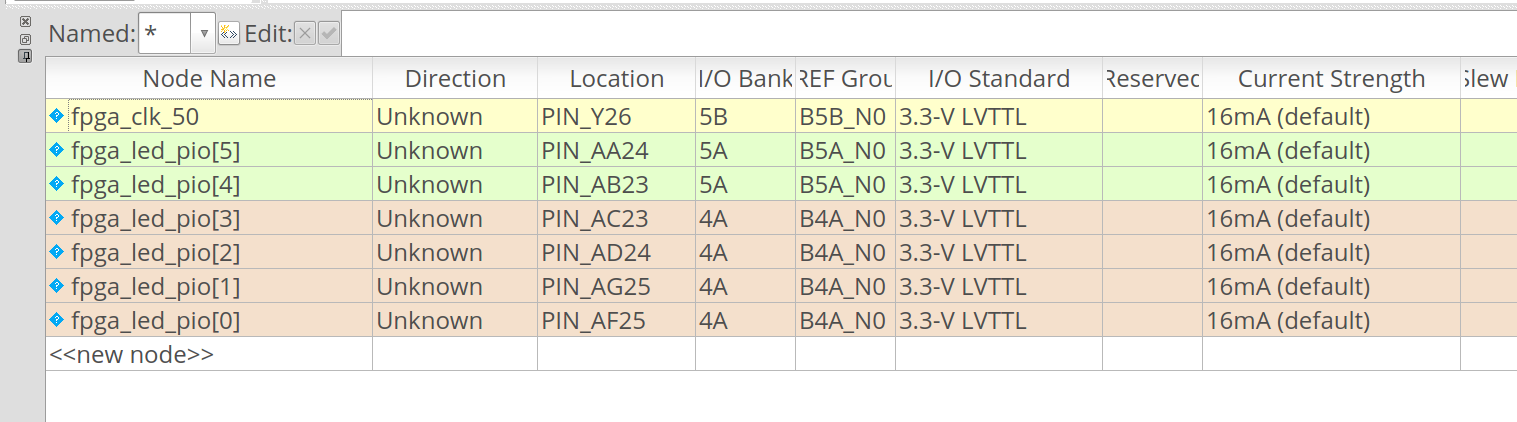
The Pin Planner interface displays the available FPGA pins/banks to be allocated to the TopLevel signals. Note that the Fitter Location column already has pins allocated to the signals, this was automatically generated by Quartus in the Filter step, however they do not correspond to the actual pins we want to use.
Exercise
Edit the Location column using the previous figure that relates the LEDs on the board with the FPGA pins.
Note:
- In our project, we only have 6 LEDs, out of the total 10 available.
- The I/O Standard does not reflect the one defined in the manual, which is
3.3V CMOS. You should change this column from2.5V CMOS (Default)to3.3-V LVTTL.
FPGA Flexibility
We normally attribute logical flexibility to the FPGA, but notice the flexibility it has in terms of defining the signal level of each pin. This gives the hardware developer countless usage options and new configurations.
Assignment Editor
Close the tool and open the Assignment Editor:
➡️ Assignments ➡️ Assignments Editor.
Note that the same information entered previously is in this editor. In fact, all FPGA configurations are displayed in the Assignments Editor, and only some in the Pin Planner.
Recompile
Recompile the project and note that there are no longer allocation errors.
The error you're encountering pertains to not having indicated the operating frequency of your system to Quartus. Since the frequency isn't defined, the Fitter and Assembler phase can't correctly optimize the project, leading to this error. Note tha in this context, "Assembler" refers to a different process than the assembler used in a program like C. For more details, refer to this resource.
Synopsys Design Constraints File (.sdc)
We need to add a new file to the project that outlines the boundary conditions of the project for the tool.
Exercise
To do this: File ➡️ New File ➡️ Synopsys Design Constraints File ➡️ Save As:
Lab1_FPGA_RTL.sdc
Exercise
Add the following content to the file:
# 50MHz board input clock
create_clock -period 20 [get_ports fpga_clk_50]

# Automatically apply a generate clock on the output of phase-locked loops (PLLs)
derive_pll_clocks
These lines instruct the tool that the signal fpga_clk_50 is a clock signal with a frequency of 50MHz (20 ns period) and to infer other automatic clocks (e.g., in case a PLL is used).
Recompile
Recompile the project and note that there are no longer any critical errors in the project.
RTL Viewer
The RTL Viewer provides a graphical way to verify if the HDL code has been correctly interpreted by the tool. It's an excellent way to check if the hardware description is correct.
Exercise
To open the RTL Viewer:
➡️ Tools ➡️ NetList Viewers ➡️ RTL Viewer.
You should see a diagrama similar to this one:

Programming
Connect the FPGA to the Host via the USB Blaster connector
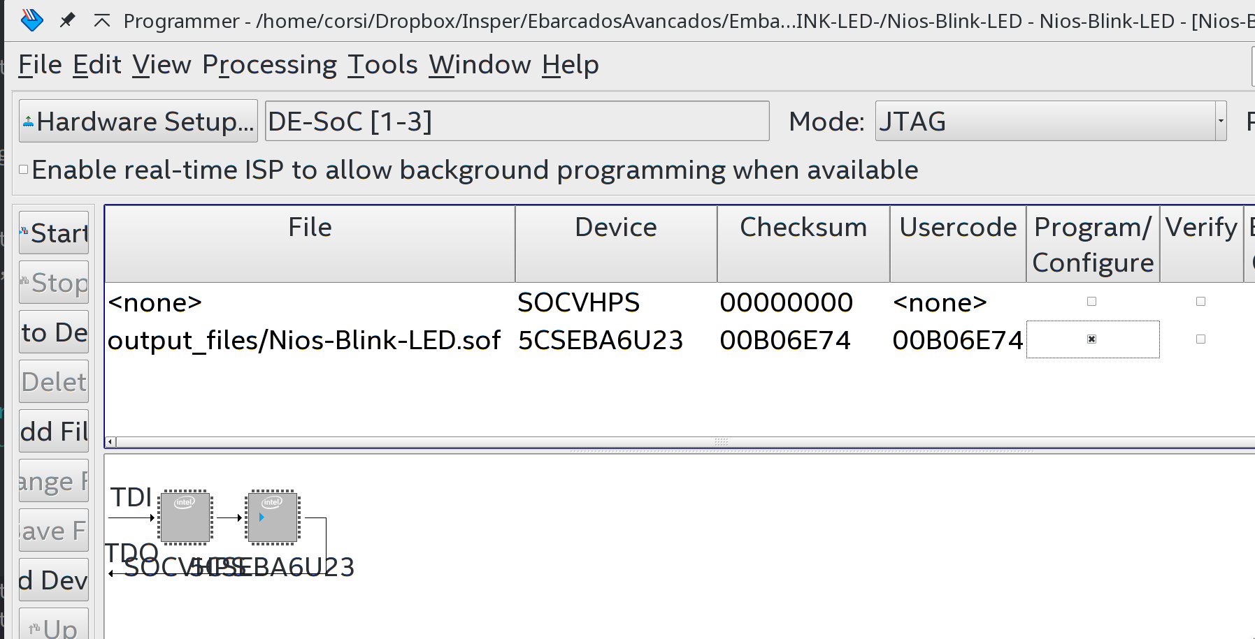
Once the project compiles, Quartus generates a binary file in the output_files folder with the *.sof extension. This file will be loaded onto the FPGA to run the project.
Exercise
To programmer the FPGA:
Tools ➡️ Programmmer.
At this stage, click on Auto Detect. This will read via JTAG all devices connected to the JTAG chain. You will notice that two devices appear:
SOCVHPS: ARM Cortex A75CSXFC6D6: FPGA
You might need to configure Linux to recognize the JTAG. Follow the steps at: Configuring USB Blaster Linux.
Exercises
Lets practical a little bit:
- 🔰 Make the LEDs blink more slowly
- 🔰 Add buttons to the project and make them control the LEDs
- Make switches control the frequency at which the LEDs blink
- Add a PWM to the LEDs to control their intensity